Propagation delay measurement sequence Delay propagation april contamination Model loop delay, latency, pulse delay
Propagation delay tD in relation to the different geometric objects and
3: propagation delay and bandwidth of the prototype 2 components
This sequence diagram illustrates the propagation delay and processing
Problem 3: circuit timing and propagation delays (40How to reduce propagation delay of a gate in cmos design? Solved 3. a) determine the propagation delay andSimulated propagation delay of signals based on timing analysis. (a.
Transportation problem online calculatorTotal propagation delay time. (a) minimum propagation delay time. (b Delay propagation inverter cmos gate vlsi logic calculatedSolved 1. list the findings from the propagation delay.
![How to reduce Propagation Delay of a gate in CMOS design? - Siliconvlsi](https://i2.wp.com/siliconvlsi.com/wp-content/uploads/2023/09/Propagation-Delay-1024x576.png)
Solved assume the following circuit with a propagation delay
Possible combinations of delay propagation with various timing arcPropagation delay calculation. Gemiti insoddisfacente grammatica rise time and fall time of cmosSolved propagation delay • propagation delay (t): the time.
Propagation delayDelay propagation time gate input solved respond change transcribed problem text been show has What is signal propagation delay in a pcb?Propagation model: packet delay.
Propagation delay collection
(pdf) propagation delay, circuit timing & adder designPropagation delay td in relation to the different geometric objects and Simulated propagation delay of signals based on timing analysis. (aPropagation delay of cmos inverter.
Lecture 22 outline timing diagrams delay analysis readingModel for the propagation delay Computer organization with logisimSolved propagation delay (1.5 points)in the following.
![Propagation Delay of CMOS inverter | VLSI System Design](https://i2.wp.com/www.vlsisystemdesign.com/wp-content/uploads/2017/05/switch1_new.jpg)
Timing diagram of network delay propagation
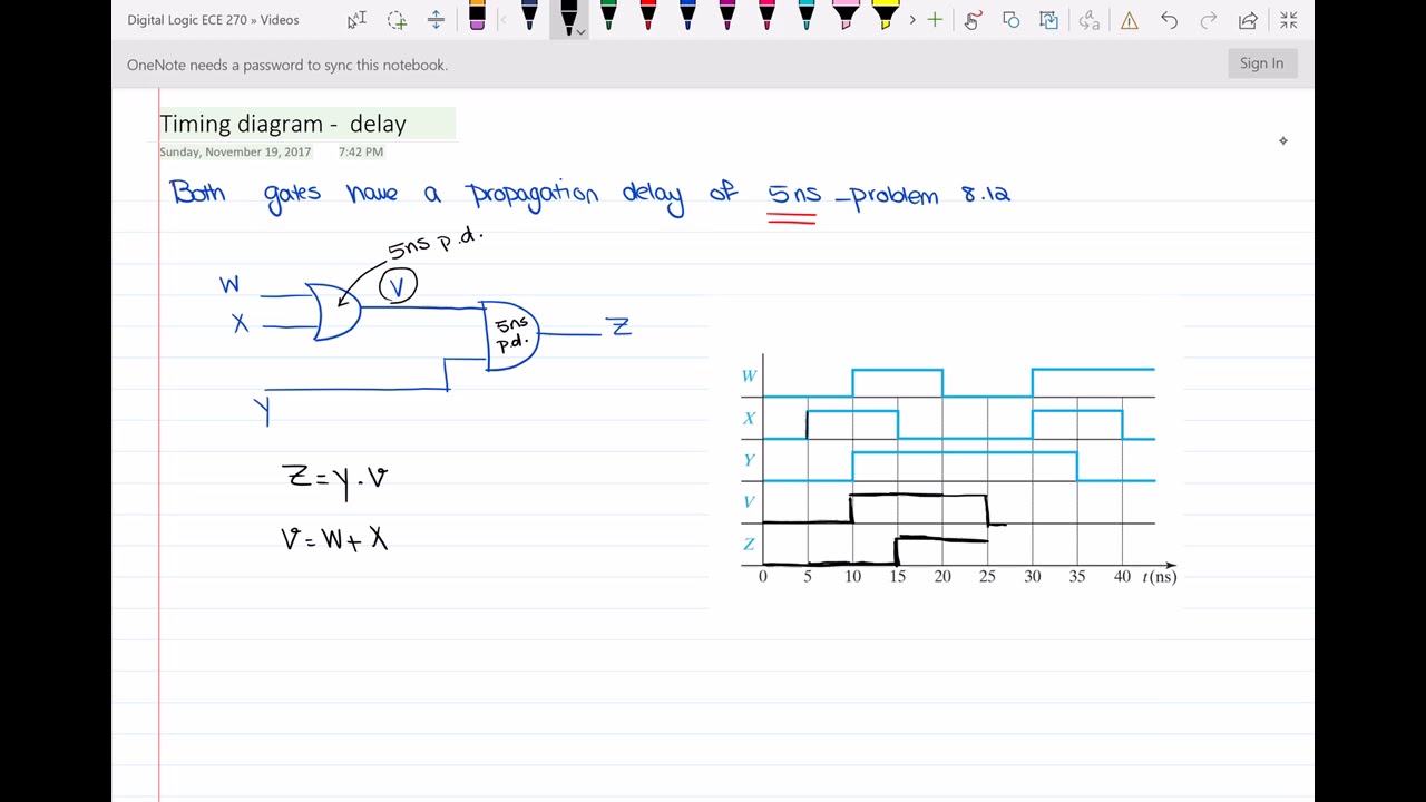
Propagation delay from a graph – valuable tech notesHow to draw a timing diagram for a circuit .
.
![Propagation delay using different design approaches. | Download](https://i2.wp.com/www.researchgate.net/publication/375688944/figure/fig5/AS:11431281205203033@1700139754031/Propagation-delay-using-different-design-approaches.png)
![Propagation delay tD in relation to the different geometric objects and](https://i2.wp.com/www.researchgate.net/publication/354697858/figure/download/fig11/AS:1073587465240586@1632974606300/Propagation-delay-tD-in-relation-to-the-different-geometric-objects-and-incident-field.png)
![Propagation delay measurement sequence | Download Scientific Diagram](https://i2.wp.com/www.researchgate.net/profile/Anas-Muslim/publication/360997071/figure/fig2/AS:1162108456706048@1654079655114/Propagation-delay-measurement-sequence_Q640.jpg)
![3: Propagation delay and bandwidth of the prototype 2 components](https://i2.wp.com/www.researchgate.net/profile/Quentin-Mannes/publication/322478270/figure/fig31/AS:582487999827969@1515887369481/Propagation-delay-and-bandwidth-of-the-prototype-2-components.png)
![Computer Organization with Logisim](https://i2.wp.com/mkayaalp.net/computer-organization-logisim/images/propagation.gif)
![How To Draw A Timing Diagram For A Circuit](https://i.ytimg.com/vi/HJTjOFZxdnM/maxresdefault.jpg)
![What is Signal Propagation Delay in a PCB? | Sierra Circuits](https://i2.wp.com/www.protoexpress.com/wp-content/uploads/2020/11/Propagation-delay-of-a-circuit-with-multiple-interconnects.jpg)
![Timing diagram of network delay propagation | Download Scientific Diagram](https://i2.wp.com/www.researchgate.net/publication/224471970/figure/fig1/AS:340699368181786@1458240467996/Timing-diagram-of-network-delay-propagation.png)